
ACAP UNSW adds Conifer single-side wafer etching system capabilities to its lab facilities
- Sep 7, 2023
- 1 min read

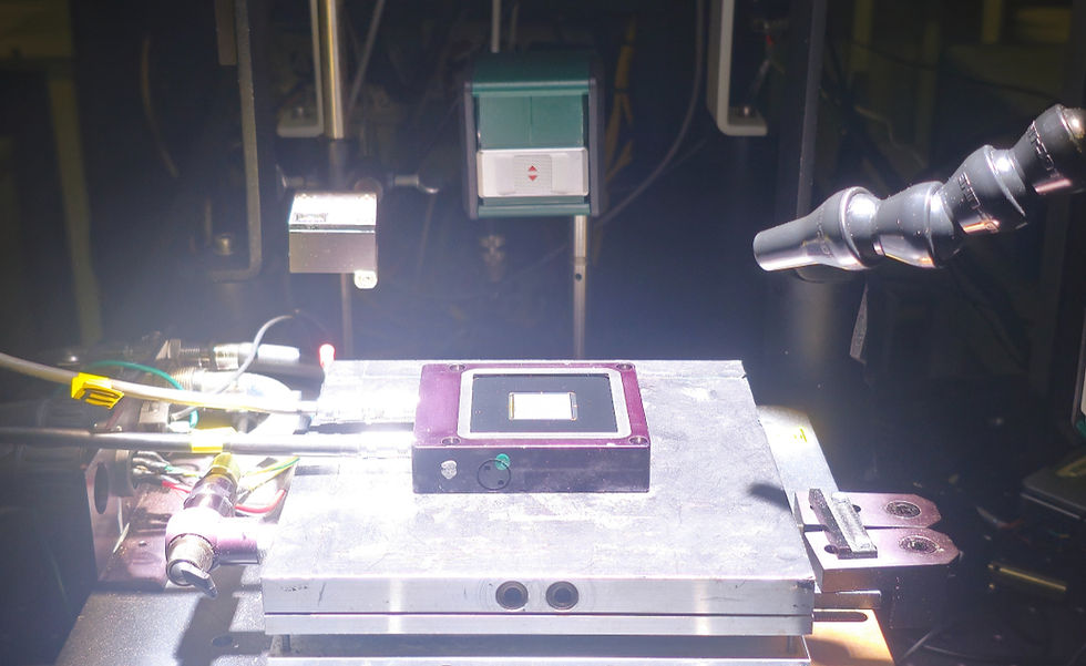
ACAP UNSW has now installed a single-side etcher for silicon wafers, in a new addition to its expanding photovoltaic research facilities.
The tool is capable of selectively etching silicon and silicon-containing wafer layers, allowing for controlled thinning of silicon wafers. When combined with existing double-sided processes, this capability allows for the development of state-of-the-art silicon solar cells, in both single-junction devices, and silicon-based tandem cells.
Emergent and future solar cell designs made for maximum power and efficiency require this range of single-sided processes, including diffusions, thin-film deposition, and texturing, as made possible by the Conifer system.

Due to surface tension, the single-side etching tool employs deionised water that forms a stable film on the wafer surface. This capping layer remains on the silicon wafer throughout the process. As the wafer moves through the etching bath, the etching solution is collected by rollers, leaving the water-protected surface of the silicon wafer untouched. Consequently, only the wafer's rear side undergoes etching.
This Conifer system also includes a cleaning and drying stage, ensuring a clean, dry, single-sided etched wafer that can be retrieved from the tool's left side. With up to 60 litres of etchant capacity, the etching depth can be regulated in a single run by adjusting the etchant type, concentration, and roller speed.

For all collaboration or partnership inquiries, please contact Bram Hoex of the Hoex Research Group at UNSW.


Comments