
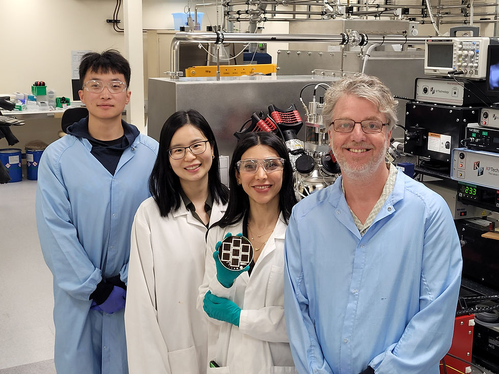
Snapshot of 2025 progress in ACAP’s Silicon solar cell research program
- Dec 22, 2025
- 2 min read

Silicon remains the reliable workhorse of the solar industry and, thanks in part to ACAP’s PP1 Silicon Solar Cells program and the silicon heavyweights in its ranks, silicon based solar technology is advancing at remarkable speed.
At the December 1, 2025 ACAP Conference held at the University of Queensland, Assoc. Professor James Bullock (University of Melbourne), Technical Program Lead for PP1, walked through how far we’ve come – and how far we can still go. This is a snapshot of what he had to share.
Today’s best large‑area crystalline silicon cells made on industry pilot lines are already hitting around 26–28% efficiency.

As James noted, the slides were barely printed before they were out of date:
“Even since I submitted these slides last week, this record here has been beaten by Jinko Solar… that’s a testament to how fast it’s moving at the moment.”
Highlighting ACAP’s impact, Bullock explained to the full auditorium at the University of Queensland, “We can actually draw a line between some of these efficiencies and the contributions made through ACAP’s research programs.”
Commercially, TOPCon cells now hold the majority market share, with heterojunction and back‑contact designs also in play. Wafer sizes are increasing, bifacial cells (that collect light from both sides) are now dominant at cell level, and modules approaching 25% are appearing in the market.

To push silicon beyond 28% cell efficiency by 2030, PP1 is focused on three big levers:
• Extracting more current from each cell
There’s still roughly an 8% relative improvement in current available compared to the theoretical limit (Jsc). PP1 teams are chasing that remaining headroom by cutting reflection and internal ‘parasitic’ losses using thinner metal fingers, back‑contact architectures, transparent contacts, and advanced light‑trapping textures (building on work presented by Professor Martin Green at SNEC).
• Holding voltage near its physical limit
Thanks to decades of work, silicon voltages are already close to their theoretical ceiling. ACAP is supporting ongoing improvements in surface passivation and wafer quality – including wafers with reduced oxygen content and astonishingly uniform quality, with implied voltages at the Auger limit across the ingot.
• Higher fill factor, less silver
New metallisation strategies are a double win: finer, lower‑resistance fingers and up to 80% less silver. One PP1 highlight combines tiny silver ‘dots’ with over‑printed copper lines, cutting silver use while keeping efficiency nearly unchanged.
Underpinning all this is the new suite of ACAP-funded fabrication and characterisation tools, and deep partnerships with companies like LONGi and Jinko, and others.
With 28% single‑junction silicon a serious target by 2030, and tailored silicon bottom cells enabling tandems approaching 40% efficiency in the next 5–15 years, silicon remains at the heart of ACAP’s push towards ultra‑low‑cost solar.


Comments